- 您现在的位置:买卖IC网 > Sheet目录316 > BUK218-50DY,118 (NXP Semiconductors)TOPFET DUAL SWITCH D2PAK
Philips Semiconductors
TOPFET dual high side switch
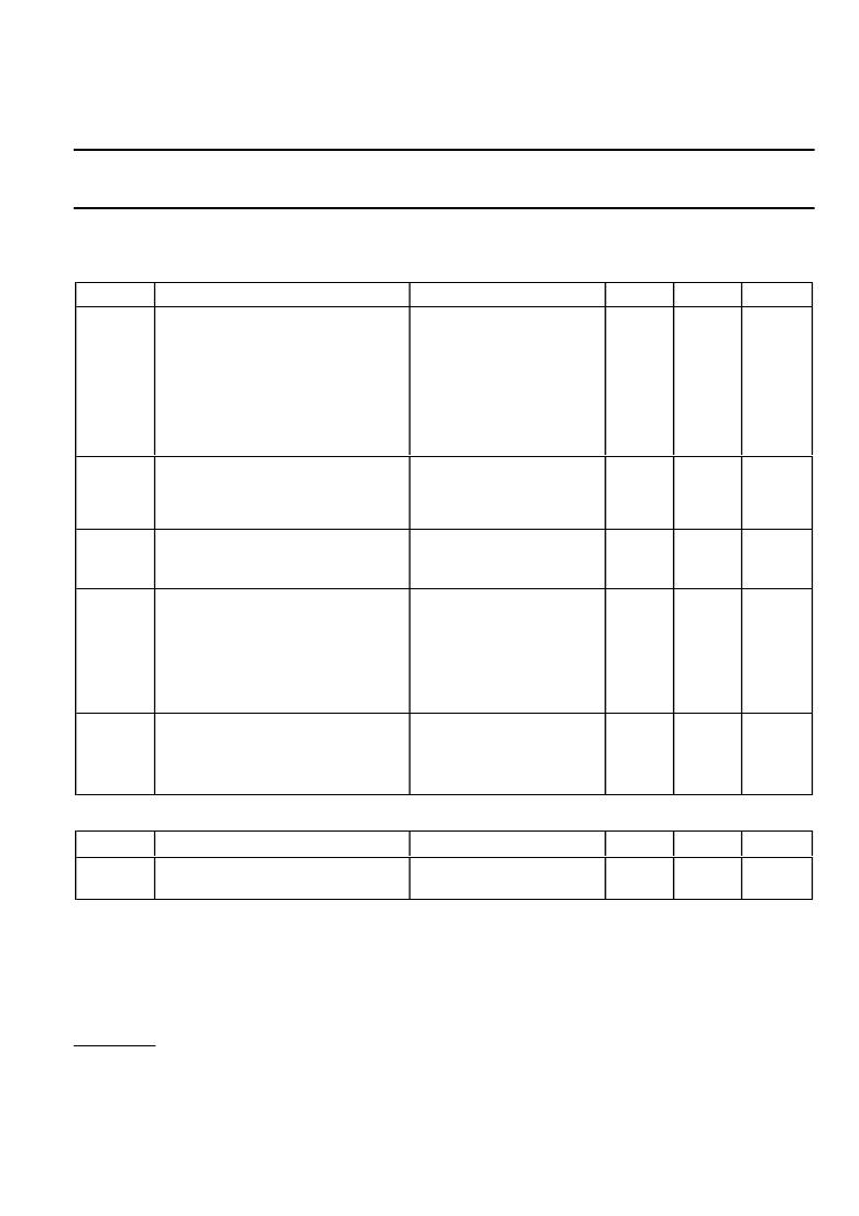
LIMITING VALUES
Limiting values in accordance with the Absolute Maximum System (IEC 134)
Product specification
BUK218-50DY
SYMBOL
V BG
I L
P D
T stg
T j
PARAMETER
Continuous supply voltage
Continuous load current per channel
Total power dissipation
Storage temperature
Continuous junction temperature 1
CONDITIONS
T mb ≤ 135?C
T mb ≤ 25?C
MIN.
0
-
-
-55
-40
MAX.
50
8
83.3
175
150
UNIT
V
A
W
?C
?C
Reverse battery voltages 2
V GB
V GB
Continuous reverse voltage
Peak reverse voltage
-
-
16
32
V
V
Application information
R I , R S
External resistors 3
to limit input, status currents
3.2
-
k ?
Input and status currents
I I
I S
Continuous input current
Continuous status current
-5
-5
5
5
mA
mA
I I
I S
Repetitive peak input current
Repetitive peak status current
δ ≤ 0.1, t p = 300 μ s
δ ≤ 0.1, t p = 300 μ s
-50
-50
50
50
mA
mA
Inductive load clamping
V BG = 13 V, I L = 8 A
E BL
Non-repetitive clamping energy (one
T j = 150?C prior to turn-off
-
150
mJ
channel)
ESD LIMITING VALUE
SYMBOL
V C
PARAMETER
Electrostatic discharge capacitor
voltage
CONDITIONS
Human body model;
C = 250 pF; R = 1.5 k ?
MIN.
-
MAX.
2
UNIT
kV
1 For normal continuous operation. A higher T j is allowed as an overload condition but at the threshold T j(TO) the over temperature trip operates
to protect the switch.
2 Reverse battery voltage is allowed only with external resistors to ensure that the input and status currents do not exceed the limiting values.
The internal ground resistor limits the reverse battery ground current. The connected loads must limit the reverse load currents. Power
is dissipated and the T j rating must be observed.
3 To limit currents during reverse battery and transient overvoltages (positive or negative).
May 2001
2
Rev 1.400
发布紧急采购,3分钟左右您将得到回复。
相关PDF资料
BVL121200003N
BATTERY CHG UNIV 12VDC @ 1.2A
BVW241250003A
BATTERY CHG UNIV 24VDC @ 1.25A
C-14245
RACKMOUNT INTERNAL CHASSIS
C-1555
CABINET SLOPING PANEL PRESTIGE
C2777-FI-J35C5-T120
CONN PLUG 35POS 0.4MM COAXIAL
C4IDCD
INPUT MODULE DC 4.5-30VDC
C4IDCK
INPUT MODULE DC 60MA 4.5-30VDC
C4OACR
OUTPUT MODULE AC C4 22MA 4-32VDC
相关代理商/技术参数
BUK219-50Y
功能描述:电源开关 IC - 配电 RAIL TOPFET2 RoHS:否 制造商:Exar 输出端数量:1 开启电阻(最大值):85 mOhms 开启时间(最大值):400 us 关闭时间(最大值):20 us 工作电源电压:3.2 V to 6.5 V 电源电流(最大值): 最大工作温度:+ 85 C 安装风格:SMD/SMT 封装 / 箱体:SOT-23-5
BUK219-50Y,127
功能描述:电源开关 IC - 配电 BUK219-50Y/SOT263/RAILH// RoHS:否 制造商:Exar 输出端数量:1 开启电阻(最大值):85 mOhms 开启时间(最大值):400 us 关闭时间(最大值):20 us 工作电源电压:3.2 V to 6.5 V 电源电流(最大值): 最大工作温度:+ 85 C 安装风格:SMD/SMT 封装 / 箱体:SOT-23-5
BUK220-50Y
制造商:PHILIPS 制造商全称:NXP Semiconductors 功能描述:TOPFET high side switch SMD version of BUK219-50Y
BUK220-50Y /T3
功能描述:电源开关 IC - 配电 TAPE13 TOPFET2 RoHS:否 制造商:Exar 输出端数量:1 开启电阻(最大值):85 mOhms 开启时间(最大值):400 us 关闭时间(最大值):20 us 工作电源电压:3.2 V to 6.5 V 电源电流(最大值): 最大工作温度:+ 85 C 安装风格:SMD/SMT 封装 / 箱体:SOT-23-5
BUK220-50Y,118
功能描述:电源开关 IC - 配电 TAPE13 TOPFET2 RoHS:否 制造商:Exar 输出端数量:1 开启电阻(最大值):85 mOhms 开启时间(最大值):400 us 关闭时间(最大值):20 us 工作电源电压:3.2 V to 6.5 V 电源电流(最大值): 最大工作温度:+ 85 C 安装风格:SMD/SMT 封装 / 箱体:SOT-23-5
BUK22150DY
制造商:NXP SEMI 功能描述:New
BUK221-50DY
制造商:PHILIPS 制造商全称:NXP Semiconductors 功能描述:Dual channel high-side TOPFET
BUK221-50DY,118
功能描述:MOSFET N-CH 50V 4A SOT427 RoHS:是 类别:集成电路 (IC) >> PMIC - MOSFET,电桥驱动器 - 内部开关 系列:TOPFET™ 标准包装:1,000 系列:- 类型:高端/低端驱动器 输入类型:SPI 输出数:8 导通状态电阻:850 毫欧,1.6 欧姆 电流 - 输出 / 通道:205mA,410mA 电流 - 峰值输出:500mA,1A 电源电压:9 V ~ 16 V 工作温度:-40°C ~ 150°C 安装类型:表面贴装 封装/外壳:20-SOIC(0.295",7.50mm 宽) 供应商设备封装:PG-DSO-20-45 包装:带卷 (TR)
